LCDs (LVDS) Bring-Up on RK3568: A Study of the Data Flow
Categories:
5 minute read
Background Knowledge
- Reference: How-to: Display Interface Debugging Standard Operating Procedure (SOP)
- Reference: Analysis of Key Concepts in the Rockchip Display Subsystem
- Example: Using LVDS as a case study
Data Flow - (Hardware Perspective)
- Okay, this step is to determine the hardware connections. Let’s directly map out the entire data flow.
1. Data from Memory -> VOP
Whether the data comes from peripherals or is on the eMMC, it must be loaded into memory. Therefore, the starting point of the data flow is memory. From memory, the data is given to the specific VP configured in the VOP. The DTS code to configure the VOP is as follows:
	&lvds_in_vp2 {
	 status = "okay";
	};
Here, VP2 is the VP that LVDS will be associated with, but this is not the case for every SoC or for every product’s application scenario.
- How-to: How do you determine which VP an interface’s data is output from?
- You must refer to this diagram from Rockchip:
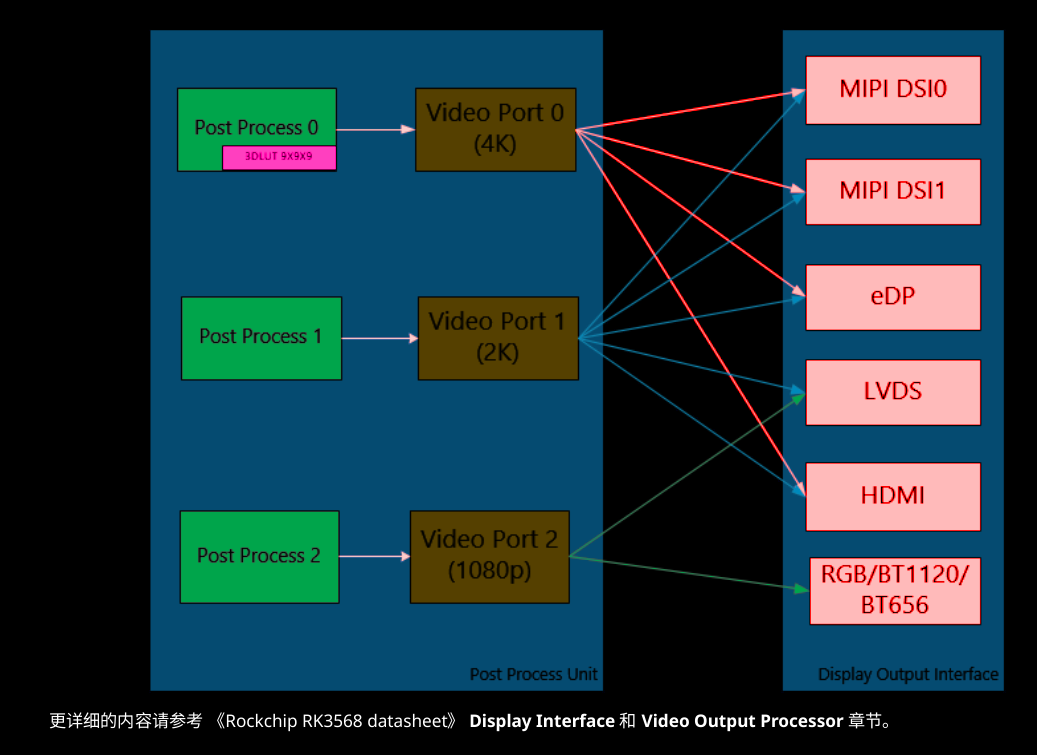
- It specifies that LVDS can only go through VP1 or VP2. Since our system requires three screens, and the performance of VP0 to VP2 decreases progressively, the frequency requirements of LVDS make VP2 the most suitable choice.
- Note here that the mention of 1080p does not mean that LVDS (as an example) can actually reach 1080p. It also depends on whether the LVDS itself is single-channel or dual-channel!
- You must refer to this diagram from Rockchip:
2. [Logical Configuration][Does Not Exist in Hardware] Signal Arrives at the route_lvds “Router”
&route_lvds {
    status = "okay";
    connect = <&vp2_out_lvds>;
};
Here, the device tree configures the router to allow a connection from LVDS.
This requires a deeper look into the internal design of the RK3568. Some might suggest that the router here is an actual IP block dedicated to connecting different display interfaces. (An “interface” here is an abstract logical concept, physically composed of a controller and a corresponding PHY, e.g., MIPI DSI Host Controller and mipi_tx DPHY). However, without concrete evidence from Rockchip’s official documentation or the chip’s technical manual to confirm the existence of this IP, it is safest to treat route_lvds as a logical concept.
- Supplement
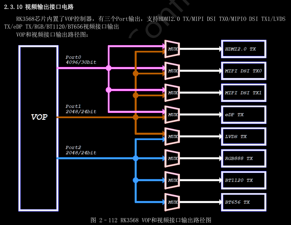
- This diagram actually provides evidence that
routeis very likely an independent IP, possibly with writable registers, which would enable the feature of routing to different display interfaces.
3. From VOP -> LVDS Controller
- In the RK3568’s design, the LVDS controller is not an independent, complex IP core like the MIPI-DSI. Its core control logic is simplified and embedded within the VOP and the GRF (General Register File). This has been deduced from the register descriptions and architectural information in the datasheet.
- It is configured through specific register bits in
GRF_VO_CONF0andGRF_VO_CONF2. You can refer to this diagram for a conceptual idea: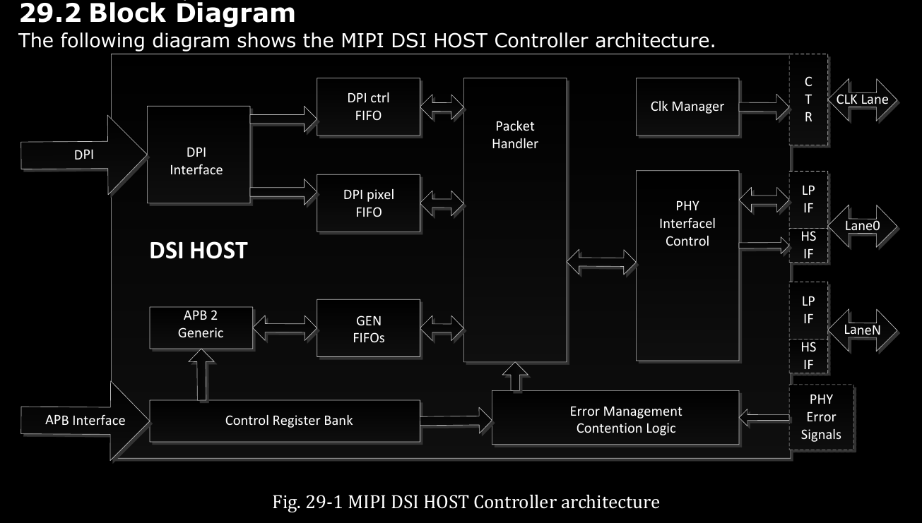
- By referencing the architecture of the MIPI-DSI controller, we can clearly see a PHY Interface Control at the end of the data flow. This indicates that the Controller’s role is to act as a “protocol converter and packer” between the VOP’s generic video data and the PHY’s physical layer. It receives RGB data from the VOP, packs it according to the LVDS bus format rules (e.g., SPWG/JEIDA), and then sends it to the PHY.
# Set in the panel node
bus-format = <MEDIA_BUS_FMT_RGB888_1X7X4_JEIDA>;
4. From LVDS Controller -> MIPI-DPHY
- In the RK3568, MIPI0 and LVDS0 share one set of PHYs, while MIPI1 and LVDS1 share another. You can refer to this table:
- The output will then follow the VP configuration in the device tree. The final output is through the pins defined in the GRF registers. These pins are the PHY’s pins, are not configurable, and will not appear as GPIOs.
- The device tree code is as follows:
- When editing the
&lvdsnode, setphys = <&video_phy0>; - And set the status of
video_phy0to"okay".$$// 2. Enable the physical layer PHY corresponding to LVDS &video_phy0 { status = "okay"; }; // 3. Complete the LVDS controller configuration &lvds { status = "okay"; phys = <&video_phy0>; };$$
- This configuration directs the LVDS signals through
phy0. Of course, in the DTS,phy0is not viewed from the perspective of a specific interface, but rather as a resource to be used—a static, objective role. The mapping between this PHY and the interface circuitry is fixed within the SoC, though it is configurable which interface uses it.
5. PHY to the LCD
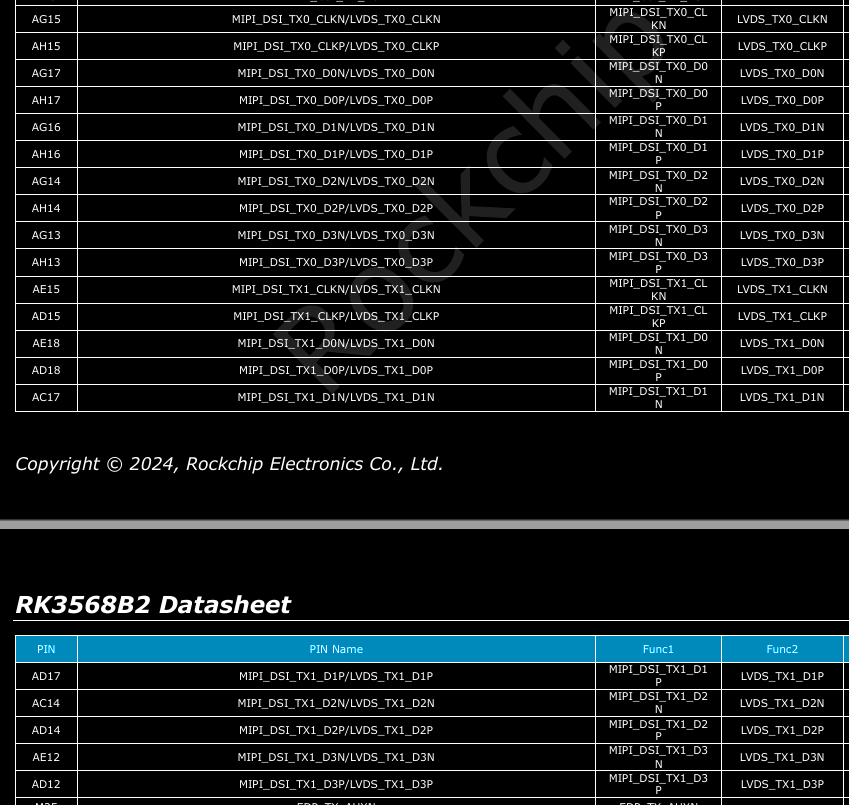
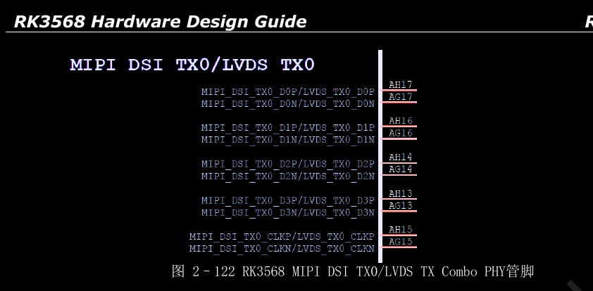 The pins in this diagram (e.g., AG17/AH17) are the pins that go directly from the PHY to the display screen, representing the final part of the data flow on the SoC side.
For an LVDS interface, there are 4 differential data pairs and 1 differential clock pair. The receiving end processes these signals according to the LVDS protocol. If everything is correct, the image from memory will be displayed.
The pins in this diagram (e.g., AG17/AH17) are the pins that go directly from the PHY to the display screen, representing the final part of the data flow on the SoC side.
For an LVDS interface, there are 4 differential data pairs and 1 differential clock pair. The receiving end processes these signals according to the LVDS protocol. If everything is correct, the image from memory will be displayed.
Summary
For this project, the target device was an FPGA, which acted as a dummy screen for me. The final resolution and frame rate successfully received by the FPGA was 1920x1080p30.
However, according to Rockchip’s official documentation, the maximum supported resolution is only 1280x800.
Therefore, it can be concluded that the LVDS controller does not impose a hard limit on hactive or vactive. More likely, as long as the clock frequency requirements are met (not exceeding the maximum limits of VP2 and the MIPI DSI TX DPHY), it is possible to push the resolution to its practical limit.
However, it’s not guaranteed that the same results can be achieved with a different screen.