GMAC Bring Up Work Flow
4 minute read
1. Identifying the GMAC from the Schematic
- From the default DTS provided by the SDK, it can be seen that there are two GMACs, gmac0 and gmac1.
1.1 First, check the schematic from the hardware engineer, search for GMAC, and see if gmac1 or gmac0 is used.
To determine this, one must look at the pins used in the schematic and compare them with the configuration of the gmac nodes in the DTS.
The specific file is located at kernel/arch/arm64/boot/dts/rockchip/rk3568-pinctrl.dtsi.
During the BSP creation process (the previous step), a layered structure was established, and this dtsi file belongs to the lowest chip-level layer. This file defines the specific sub-nodes of gmac1, and which pins correspond to each sub-node, for example:
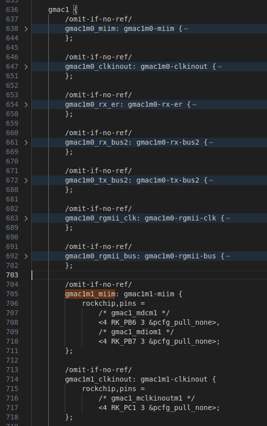
When it comes to gmac1, it is further divided into m0 and m1. The image I have captured is the m1 portion. How do we know to use m1? We can refer to the CPU section of the schematic:
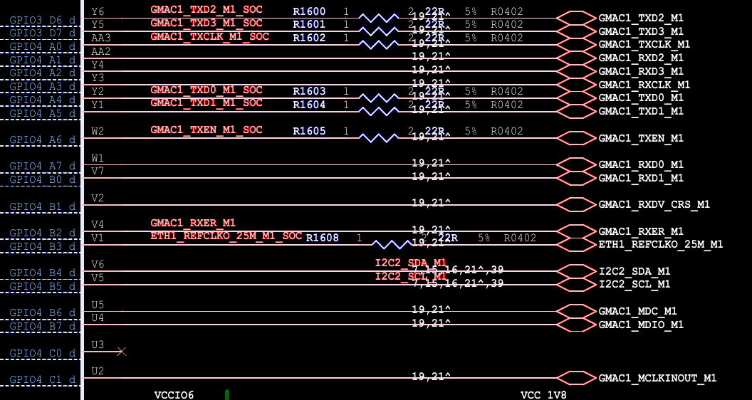
I have specifically captured the gmac module used this time. The hardware engineer has added “M1” after each pin name, which also reminds us that the one being used is GMAC1’s M1.
1.2 Actually, why can the hardware side correspond to the DTS?
It is likely because when the hardware engineer was designing the schematic, they directly referenced the usage guidelines provided by the Chip Manufacturer. It’s divided into GMAC1 and GMAC0, and GMAC1 is further divided into M0 and M1. I would guess that if we insisted on modifying it, using a hybrid version like a GMAC2 wouldn’t be entirely impossible, but the DTS side would have to be completely redone. We would have to write out each pin one by one, just as it’s done in kernel/arch/arm64/boot/dts/rockchip/rk3568-pinctrl.dtsi.
1.3 To summarize:
Looking at the symbols in the schematic is just a tip and not definitive. The definitive way is to compare the pins configs in the chip-level dts include file. They must correspond.
2. Determining the Clock Mode from the Schematic, and the flow of 25M and 125M clocks
2.1 First, look at the PHY section of the schematic
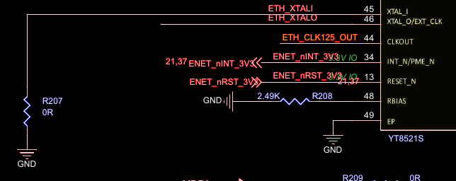
Here we can see that XTAL_I is grounded, and we don’t yet know where XTAL_O and CLKOUT are connected.
2.2 Look at the PHY’s DataSheet
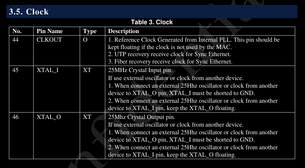
2.2.1 First, look at No.44
It is specifically written here that CLKOUT is an output type, and if it’s not needed to output a clock to the MAC, this pin should be left floating.
However, it is not floating here, so the schematic must be outputting a 125MHz clock to the MAC.
2.2.2 Next, look at No.45
It is introduced here that if XTAL_O is supplied with an external 25MHz clock, then XTAL_I must be grounded. So, from the schematic showing XTAL_I is grounded, it should mean an external 25MHz is being supplied to the PHY.
Therefore, we just need to further trace which pins are actually connected.
3. Enter the dts directory, find the entry dts, disable redundant devices, and enable the target device
Because GMAC1M1 is used on my board, GMAC0 can be disabled.
/*
* 2nd: Configure the active GMAC0 interface.
*
* NOTE:   The properties below are overrides for the &gmac0 node,
*         which inherits its base configuration from "rk3568-evb1-ddr4-v10.dtsi".
*
* ACTION: Review these settings against your schematic.
*/
&gmac0 {
	// there is more ...

	//status = "okay";
	status = "disabled";
};

&mdio0 {
	status = "disabled";
	// there is more ...
};
My initial judgment was not to use gmac0, so I did a lot of debugging, and only at the very end did I change them all to status = "disabled";
4. Open Rockchip_Developer_Guide_Linux_GMAC_Mode_Configuration_CN.pdf
Based on the determined clock mode, directly copy the node configuration. Do not modify other dtsi files (they are just libraries).
Open this manual provided by Rockchip:
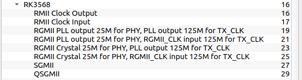
There are so many modes here. SGMII, which stands for Serial Gigabit Media Independent Interface, is used for bridging, so SGMII and QSGMII are not within my scope of concern.
RMII Clock Input and Output also don’t seem to apply to the current board’s situation, because I have two clock speeds, 25MHz and 125MHz, so I’ll look at the other four modes first.
Here, I referenced an article by an engineer named Baron:
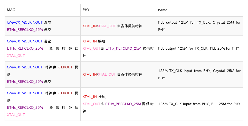
Reference Link: A very good article
Following this summary, we should now choose RGMII PLL output 25M for PHY, RGMII_CLK input 125M for TX_CLK.
5. Summary
The above is just the normal porting process. During bring-up, it is very likely that the hardware is not okay. So, after confirming the correct porting process, you can confidently proceed to find bugs in the hardware.
Regarding the debugging mindset, my personal notes are organized here to provide a starting point for thinking: GMAC Bring-Up Debug Strategies